PUBLICATIONS
Recent publications on research, applications and methods
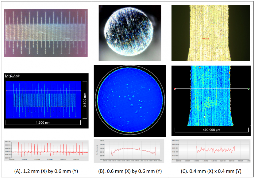
A solution to the sub-micron dimensional measurement of nominal flat high precision components is presented. The system comprises a calibrated X,Y motion system with vertical confocal point sensing. The measurement data is a standard 2.5D format. The system developed is tested for repeatability and accuracy on a calibration artifact developed for the purpose. The system described addresses the measurement of components better than the current accuracy and precision of conventional coordinate measurement machines (CMM’s). Results are presented for the system in a normal office environment. The results show a precision in dimensional characterisation of better than 50 nm. The results demonstrate a solution for high precision (nanometre repeatability) dimensional component metrology.
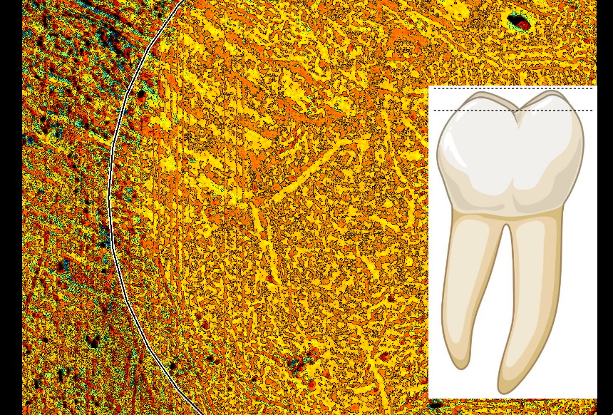
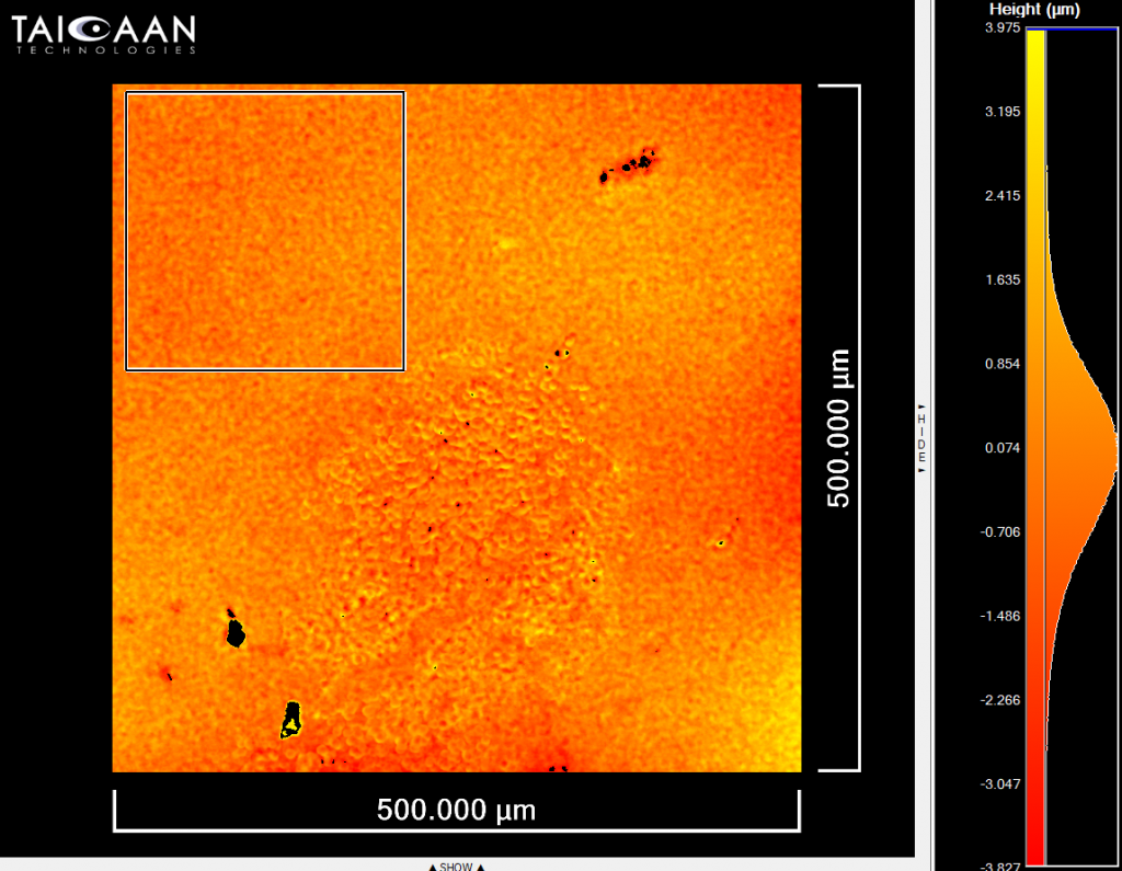
A partial human natural unprocessed dental sample was submerged in Citric Acid (0.3% pH.3.2), for 1 hour, without agitation, over a selected region (diameter 1.5 mm). The sample was measured using the TaiCaan XYRIS 2020 H instrument “before and after” the test and measured using X-Ray CT (XCT) in the “after” condition, for direct comparison with the optical measurement. The analysis of the sample was conducted using a 80 μm 3D gaussian filter to remove the surface form while maintaining the surface roughness. The 3 surfaces were compared and co-located to allow comparison of 3D surface roughness (Sa). A square region (0.6 x 0.6 mm) of the surface is segmented into 16 measurement regions (0.15 x 0.15 mm) and the roughness of each region compared. Results demonstrate that the “after” optical measurement shows a reduction of surface roughness proportional to the initial roughness of the surface. A comparison with the “after” XCT indicates a similar result to the optical data with a further reduction in roughness values when compared to the optical.
An automated in-situ electrical contact evolution (ICE) apparatus is described, the system allows the study of electrical contact performance at low contact force (<2 mN) MEMS/NEMS switching applications. The ICE system is built around a granite metrology frame and combines the controlled switching of surfaces with the ability to measure surface wear. This is achieved using a high precision motion system to move between the switching and the surface measuring positions. The surface is measured using a confocal optical sensor to provide a measurement of 3D surface wear. In this paper we describe an improved ICE system with the ability to measure both static contact force and dynamic force during the switching process. A key requirement of the new system is the ability to measure adhesion forces between opening contacts. In this study a Gold coated hemisphere (radius 1 mm) is used with a Gold Coated (500 nm), multiwalled forest of vertically aligned carbon nanotubes (50 μm), referred to as Au/CNT. The system has been designed to allow a range of contact materials to be tested, providing a unique testing platform that combines the evaluation of switching performance and contact resistance measurement with the ability to monitor surface wear.
This paper focuses on the verification of computational modelling of arc motion under short circuit conditions in low voltage circuit breakers using controlled experimental conditions, where an arc imaging system (AIS) is used to provide quantitative information on arc motion. It is shown that the motion of an arc root on a metallic surface, is linked to the arc voltage and that the computational model provides a representation of the overall arc movement, but is unable to predict high frequency events (1 MHz) associated with the arc entry into splitter plates and re-strikes within the arc chamber. To enable a prediction of arc voltage prior to extinction, referred to as the arc exit voltage, a modification to the arc model is shown and discussed with reference to the observed information from the AIS.
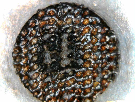
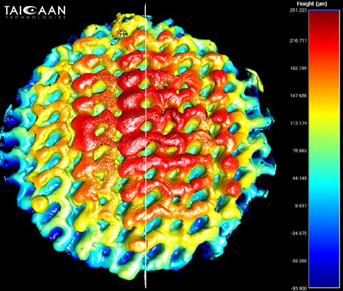
The characterisation of a highly structured surface is explored. The surface investigated has both high aspect ratio and hidden features. A regular AgNi (80/20) electrical contact has been structured using a scanning electron-beam, with the objective of wear reduction during arcing events. An X-Ray Computed tomography system (XCT) is used to provide data of the whole surface and the data then referenced against a standard calibrated high gauge confocal optical surface metrology system using standard surface metrology software. To allow the surface analysis of the XCT data, the workflow and associated data processing steps are described. The results show that the XCT method provides surface data on the whole surface area including the hidden features, but that the data resolution and associated uncertainty, limits the accuracy of the roughness evaluation. The full surface area is determined using a combination of optical and XCT data.
XYRIS 3D Non-Contact Profilers use a chromatic light-based technology to measure any material surface: transparent, opaque, specular, diffusive, polished or rough. Unlike a touch probe technique, the non-contact technique can measure inside tight areas and will not add any intrinsic errors due to deformation caused by the tip pressing on a softer plastic material. Chromatic light-based technology also offers superior lateral and height accuracies compared to focus variation technology. XYRIS Profilers can scan large surfaces directly without stitching and profile the length of a part in a few seconds. Nano through macro range surface features and high surface angles can be measured due to the profiler’s ability to measure surfaces without any complex algorithms manipulating the results. This report provides users with an understanding of the technology and the data format. The information is essential to all users of XYRIS instruments and the accompanying software analysis package BEX®

